

TSMC has unveiled the next leap in semiconductor technology, one that will take us beyond the 1nm: CFET
TSMC has unveiled its next-generation transistor architecture: the Complementary Field-Effect Transistor (CFET), marking a significant step beyond the 1nm process node. This advancement promises to redefine transistor scaling, performance, and energy efficiency, setting the stage for future semiconductor innovations.
Table of Contents
- Introduction
- What is CFET?
- TSMC’s CFET Milestone
- Advantages of CFET Technology
- Challenges Ahead
- Implications for the Semiconductor Industry
- Top 5 Frequently Asked Questions
- Final Thoughts
- Resources
Introduction
As the semiconductor industry approaches the physical limits of traditional transistor scaling, innovative architectures are essential to sustain performance improvements. TSMC’s introduction of CFET technology represents a pivotal development in this context, offering a pathway to continue Moore’s Law beyond the 1nm threshold.
What is CFET?
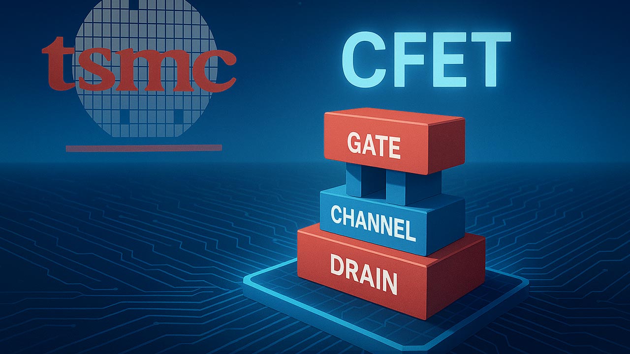
Complementary Field-Effect Transistors (CFETs) are an advanced transistor architecture that vertically stacks n-type (NMOS) and p-type (PMOS) transistors. This design contrasts with traditional planar or FinFET structures, where transistors are placed side by side. By stacking the transistors, CFETs significantly reduce the footprint of logic gates, enabling higher transistor densities and improved performance.
TSMC’s CFET Milestone
At the IEEE International Electron Devices Meeting (IEDM) in December 2024, TSMC presented its progress in CFET development. The company demonstrated a monolithic CFET inverter with a 48nm gate pitch, equivalent to a 5nm process node. This inverter features stacked n-type and p-type nanosheet transistors with backside contacts, achieving a voltage transfer up to 1.2V and subthreshold slopes between 74 and 76mV/V for both transistor types. While this marks a significant milestone, TSMC acknowledges that the technology is not yet ready for commercial production.
Advantages of CFET Technology
- Increased Transistor Density: By stacking NMOS and PMOS transistors, CFETs effectively double the transistor density compared to traditional planar designs.
- Enhanced Performance: The reduced gate length and improved electrostatic control in CFETs lead to faster switching speeds and better overall performance.
- Lower Power Consumption: CFETs offer improved energy efficiency due to reduced parasitic capacitance and leakage currents.
- Scalability: The vertical architecture of CFETs provides a scalable path for future technology nodes beyond 1nm.
Challenges Ahead
Despite the promising advantages, several challenges must be addressed before CFETs can be commercialized:
- Fabrication Complexity: The vertical stacking of transistors requires precise alignment and advanced fabrication techniques.
- Thermal Management: Managing heat dissipation in densely packed vertical structures is more complex than in planar designs.
- Material Integration: Developing suitable materials that can withstand the fabrication process and maintain performance is critical.
- Design Methodologies: New design tools and methodologies are needed to fully leverage the benefits of CFET architecture.
Implications for the Semiconductor Industry
TSMC’s advancement in CFET technology signifies a critical step in sustaining Moore’s Law and meeting the growing demands of high-performance computing, artificial intelligence, and other data-intensive applications. As the industry moves toward sub-1nm nodes, CFETs offer a viable solution to overcome the limitations of traditional transistor architectures.
Top 5 Frequently Asked Questions
Final Thoughts
TSMC’s development of CFET technology marks a significant milestone in semiconductor innovation. By addressing the limitations of traditional transistor architectures, CFETs pave the way for continued advancements in computing performance and energy efficiency. As research progresses, CFETs are poised to become a cornerstone of future semiconductor technologies.


Leave A Comment